We have received many requests for SigNASII since its release in September 2010, and many customers have been using it. Among them, one of the most common requests was "to test a large amount of NAND flash memory at once for acceptance testing.
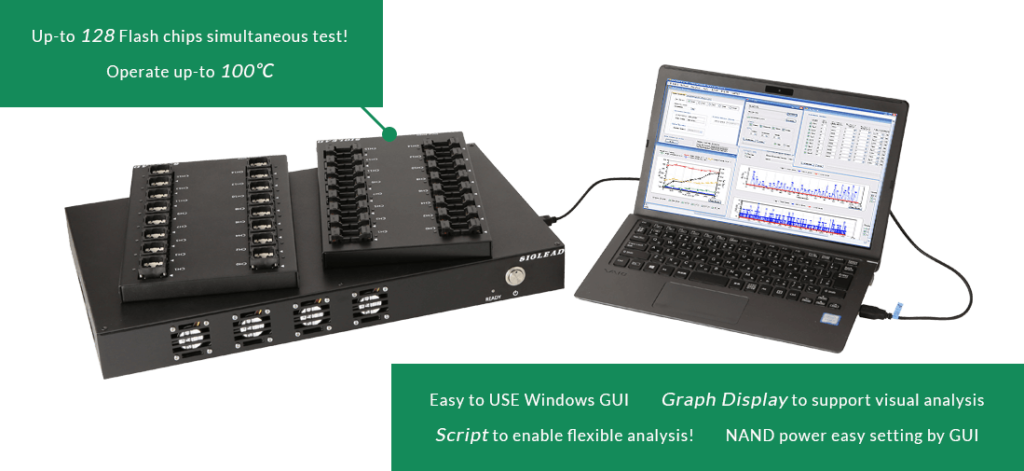
Developed from the base of SigNASII and with the same analysis functionality, SigNAS3 delivers testing on up to 128 NAND flash simultaneously. This gives SigNAS3 the capability of conducting a wide range of tests on massive numbers of NAND flash in a short period of time. Tests such as acceptance inspection, NAND sorting, reliability evaluation, cycling tests, error cause investigation (data retention, program disturb, read disturb) analysis, access time tests, etc. can be done very quickly.
SigNAS3 supports different NAND interfaces, such as SDR, Toggle DDR, Toggle DDR2.0, NV-DDR and NV-DDR2 etc. Also, it has been confirmed to work with all NAND type SLC/MLC/TLC for the latest processes, such as Toshiba 19nm, Micron/Intel 20nm and Samsung 21nm.
Summary
SigNAS3 is an easy-to-use NAND analyzer system, suitable for testing massive numbers of NAND (up-to 128) simultaneously. Various tests such as acceptance inspection, operation verification, cycling tests, access time tests, error investigation, error cause analysis and ECC evaluations can be easily done quickly. It can be used for NAND sorting judged by bit error rate/page error rate; tests on bit error caused by data retention, program disturb and read disturb; and error distribution.
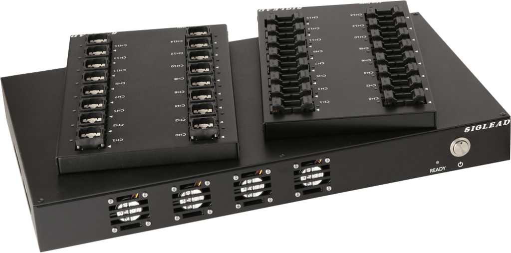
SigNAS3 is composed of the main-board with FPGA-based NAND controllers, the sub-board(s) where NAND flash for tests is set up, and Windows-based software.
Features
1. Main-board (Sp3993)
- Up-to 8 Sub-boards are connectable
- Indicates communicating status of NAND/PC by LED
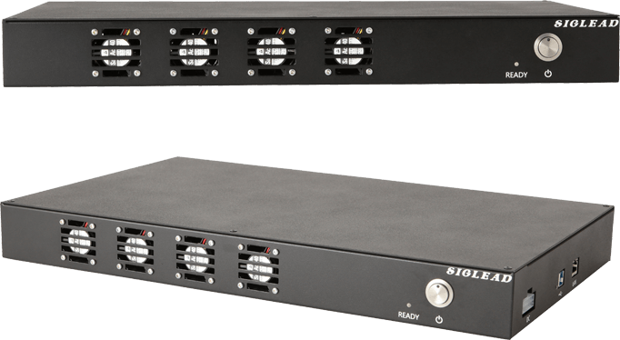
Product Specifications
| Size | Main-board : 284.5mm x 478.5mm x 51.5mm Sub-board : 279mm x 170mm x 45mm |
|---|---|
| Power Supply | AC:90V~264V (DC:15V/40A) |
| Power Consumption | 360W *in case of fully loaded: i.e. 8-sub-boards are used |
| Storage temperature | Main-board : -40~105degC Sub-board : -40~105degC |
| Operating temperature | Main-board : 0~55degC Sub-board : -40~100degC |
| NAND testing number | up-to 128 *in case of fully loaded: i.e. 8-sub-boards are used |
| I/F | USB2.0, USB3.0, Giga Ethernet |
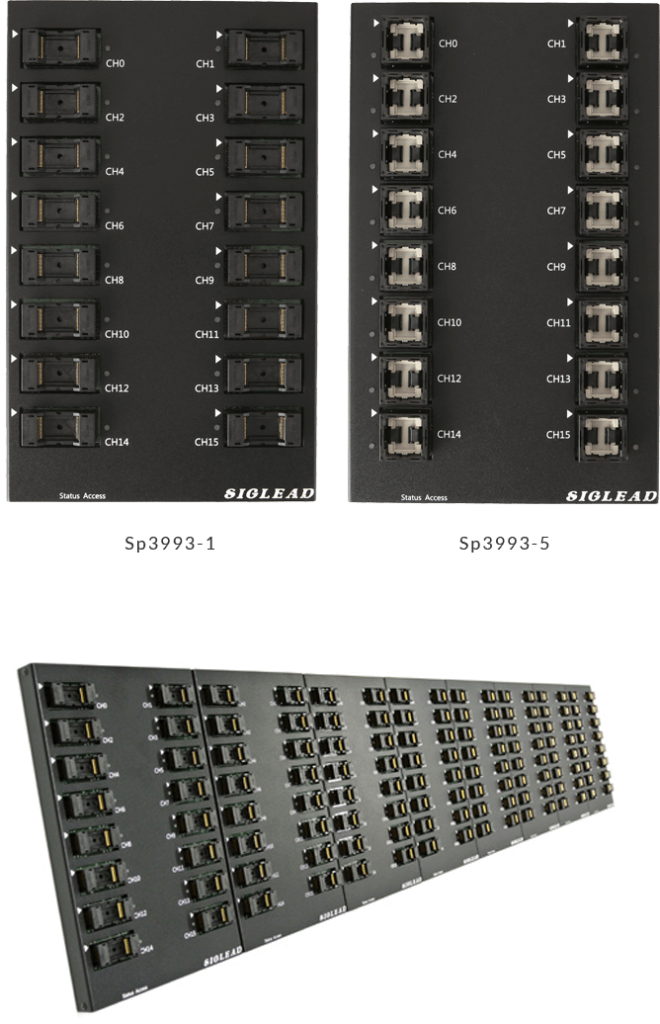
2. Sub-board (Sp3993-x)
- Up-to 16 NAND flash could be set-up for each.
- Can be connected to main-board by cable with up to 2 meter length (standard cable length is 1 meter).
- Power supplied by main-board via cable
- Power Switch ON/OFF is controlled independently for each sub-board
- Power supply of NAND flash can be controlled from PC software.
Sub Board Lineup
| Product No. | Socket |
|---|---|
| Sp3993-1 | TSOP48 |
| Sp3993-2 | BGA132 |
| Sp3993-3 | BGA63 |
| Sp3993-4 | BGA100 |
| Sp3993-5 | BGA152 |
| Sp3993-6 | BGA272 |
| Sp3993-7 | BGA316 |
3. Testing software
【Testing software enables: (part of features)】
- Set NAND interface timing
- Set NAND device power voltage
- Get NAND ID/Status
- Bad Block scan/management
- Access time test
- Access time as the function of P/E cycles
- Issue NAND command (Erase Program, Read)
- Set program pattern (Increment, Pseudo Random, Page Stripe, etc)
- Dump & save read data
- P/E Cycles (cycle number, program pattern are programmable)
- Support script language (SIGLEAD Script Language; SSL)
- Programmable ECC strength
- Data retention test (time vs. bit error)
- Program disturb test (P/E cycles Vs bit error)
- Error distribution (by page/column)
Supported NAND
| Toshiba | Samsung | Micron | Hynix | SanDisk | |
| SLC | ✔️ | ✔️ | ✔️ | ✔️ | ✔️ |
| MLC | ✔️ | ✔️ | ✔️ | ✔️ | ✔️ |
| TLC | ✔️ | ✔️ | ✔️ | ✔️ | ✔️ |
| 3D NAND | ✔️ | ✔️ | ✔️ | ✔️ | |
| Async./SDR | ✔️ | ✔️ | ✔️ | ✔️ | ✔️ |
| Sync./Toggle DDR | ✔️ | ✔️ | ✔️ | ✔️ | ✔️ |
| RR | ✔️ | ✔️ | ✔️ | ✔️ | |
| Prosess | 15nm | 14nm | 16nm | 16nm | 15nm |
- ONFI 4.1 / Toggle DDR 2.0 compliance devices (SLC / MLC / TLC / 3D)
- NAND Interface : SDR (Asynchronous) / NV-DDR (Synchronous) / Toggle DDR
- Package : TSOP 48pin, BGA 63pin/100pin/132pin/152pin/272pin/316pin
- Confirmed latest NAND: Toshiba 15nm, Micron/Intel 16nm, Samsung 14nm
- System adjustment can be done to resolve the case that NAND doesn't work
Technical support
- 1 year technical support (via telephone and email)
- 1 year free version update/bug-fix of testing software
- For support after 1 year since purchase, an extra support contract is needed
Deliverables
Deliverables consist of the following parts. Immediate analysis can be carried out at the date of delivery.
<Main-board set (Sp3980) >
- Main-board (Sp3993)
- - Power unit
- - Analysis software
- - NAND controller circuit and firmware
- - Operational Guide *USB cable and LAN cable are not included
< Sub-board set (Sp3980-x)>
- Sub-board (Sp3993-x)
- Cable (standard length is 1m, 2m max)
For more information/customization on NAND flash memory tester, please contact us.
The content might change without a previous notice due to the improvement.